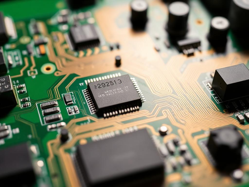
PCB 101: What a PCB Is, How to Judge Quality, and How to Specify a Good Board (with a practical checklist)
Printed Circuit Boards (PCBs) are the structural and electrical backbone of electronic products. A PCB mechanically supports components and provides the copper interconnects that route power and signals. Getting the PCB right affects everything—signal integrity, thermal behavior, reliability, compliance, and total cost.
Below is a comprehensive, practical guide you can use to understand PCBs, judge quality, and write a production-ready specification—plus how MorePCB.com fits from prototype to volume.
What is a PCB?
Layers & stack-up. A PCB is a sandwich of copper foils and insulating laminates (typically FR-4 epoxy-glass). Boards range from 1–2 layers (simple) to 4–10+ layers (mixed-signal, RF, high-speed), and into HDI (high-density interconnect) with microvias.
Key elements
- Substrate: FR-4 (most common), high-Tg FR-4, RF/low-loss materials (PTFE, hydrocarbon/ceramic), aluminum/copper cores (MCPCB) for LEDs/thermal.
- Copper weight: 0.5 oz/ft² (17 μm), 1 oz (35 μm), 2 oz (70 μm) or more for power.
- Dielectrics: Prepregs/cores set electrical spacing and impedance.
- Surface finish: HASL (lead-free), ENIG (flat, solderable, great for fine pitch), ENEPIG (wire-bond), OSP, ImmAg, ImmSn.
- Solder mask & silkscreen: Protection and labeling.
- Vias: Through-hole, blind/buried, microvias (laser).
Common PCB Types & When to Use Them
| Type | Use case | Why choose it |
|---|---|---|
| 2-Layer FR-4 | Hobby, simple controllers | Lowest cost, quick turns |
| 4-Layer FR-4 | Mixed-signal, MCU + RF | Solid GND plane, cleaner return paths, better EMC |
| HDI (microvias) | Compact, fine-pitch BGA/SoC | High density routing, smaller boards |
| Rigid-Flex / Flex | Wearables, portable medical | Reliability in motion, space saving |
| MCPCB (metal core) | High-power LEDs, drivers | Excellent heat spreading |
| RF/Low-loss | Antennas, mmWave, Wi-Fi front-ends | Controlled, low-loss transmission |
How to Evaluate a "Good" PCB (Quality Signals)
- Materials fit the job
- Correct Tg (≥ 150–170 °C for reflow/thermals).
- Low-loss dielectric for high-speed/RF when needed.
- Stack-up integrity
- Documented layer order, dielectric thicknesses, target impedance (e.g., 50 Ω single-ended, 90/100 Ω differential) with real-world tolerances.
- Manufacturability
- Realistic trace/space (e.g., 4/4–6/6 mil for standard; 3/3 for HDI).
- Via choices matched to capability (PTH vs microvia; annular rings ≥ 4–5 mil typical).
- Surface finish
- ENIG for fine-pitch/BGAs and probe durability; HASL-LF for low cost.
- Clean solder mask & registration
- Mask not encroaching pads, proper expansion; crisp silkscreen.
- Drilling & plating quality
- Uniform plating thickness, minimal hole wall roughness; via fill consistency (if specified).
- Flatness & warpage
- Within IPC limits (important for pick-and-place, BGAs).
- Dimensional accuracy
- Outline within tolerance; slots, cutouts, and panelization correct.
- Documentation & traceability
- Lot IDs, date codes, material certificates, test coupons, impedance reports (if requested).
- Inspection & test
Must-Know Standards (good boards align with these)
- IPC-6012 (Qualification and performance specification for rigid PCBs)
- IPC-A-600 (Acceptability of PCBs)
- IPC-2221/2222 (Generic & sectional design standards)
- IPC-7351 (Land pattern design)
- RoHS/REACH environmental compliance
For medical/industrial/aerospace builds, workmanship often targets IPC Class 2 or Class 3 (high reliability).
Manufacturing Flow (what happens to your files)
- CAM review (DFM): checks clearances, drill, mask, silkscreen, copper thieving, impedance.
- Imaging & etching: copper patterns defined.
- Lamination: multilayers pressed under heat/pressure.
- Drill & plating: holes drilled, copper plated.
- Solder mask & finish: apply mask, then ENIG/HASL/etc.
- Profiling: route/laser cut the outline, V-cut if panelized.
- Electrical test: nets verified against your data.
- Final QA: AOI, visual, packaging with desiccant/humidity cards if needed.
Electrical & Reliability Considerations
- Signal integrity (SI): correct impedance, short return loops, matched lengths on high-speed pairs, minimal stubs.
- Power integrity (PI): low impedance PDN, decoupling strategy, copper pours, thermal reliefs near power.
- Thermal: copper weight, heatsinks/thermal vias, MCPCB for LEDs.
- EMC/EMI: continuous ground planes, stitching vias, controlled edge rates.
- Creepage/clearance: meet safety distances (especially mains/medical).
- Conformal coating/potting: for harsh or humid environments.
Visual & Functional Defects to Watch
- Solder mask over pads, under-etch/over-etch, mask mis-registration
- Pinholes/voids in plating, poor via fill, barrel cracking
- Burrs on edges/slots, warpage beyond spec
- Impedance out of tolerance on controlled lines
If you specify acceptance criteria (IPC class), thicknesses, finish, and test, you'll filter most issues before they matter.
Cost Drivers (what makes boards expensive)
- Layer count and overall size/thickness
- Tight rules (trace/space, annular ring), microvias/HDI
- Exotic materials (low-loss RF, polyimide)
- Surface finish (ENIG/ENEPIG > HASL/OSP)
- Special features (controlled impedance, back-drill, edge plating, castellations)
- Yield risk (very fine pitch, many drill sizes)
Optimize early: agree on a manufacturable stack-up and design rules with your fabricator.
A Practical Spec Template (copy/paste and edit)
Board: 4-layer FR-4, Tg ≥ 170 °C
Outline: 85 × 55 mm, ±0.1 mm
Copper: 1 oz outer, 0.5 oz inner
Stack-up: L1 Signal / L2 GND plane / L3 Power plane / L4 Signal
Dielectrics: to achieve 50 Ω SE / 100 Ω DIFF ±10% (report required)
Rules: 4/4 mil trace/space, via drill 0.2 mm, annular ring ≥ 0.1 mm
Vias: PTH; tenting on outer layers; via-in-pad only where marked (filled & capped)
Finish: ENIG (Ni/Au)
Mask/Silk: Green mask, white silkscreen; 3 mil mask expansion
Testing: 100% electrical test; impedance coupon and report
Quality: IPC-6012 Class 2 (Class 3 for safety-critical)
Docs supplied: Gerbers RS-274X, Excellon drills, BOM (if assembly), Pick-and-Place, readme with notes

Receiving Inspection Checklist
- ✅ Packing dry-pack (if required), labels, lot/date code
- ✅ Dimensions & hole sizes per drawing
- ✅ Mask registration, silkscreen clarity, finish uniformity
- ✅ Warpage within IPC spec
- ✅ Electrical test passed; impedance report within tolerance
- ✅ No exposed copper where none expected; edges smooth
How MorePCB Helps (prototype → production)
- Design-for-Manufacturability (DFM) review of Gerbers & stack-ups to catch rule conflicts early.
- Capabilities: 1–50 layers, HDI (down to 3/3 mil typical), rigid-flex, MCPCB, controlled impedance, ENIG/ENEPIG/HASL-LF.
- Assembly (PCBA): SMT/THT, fine pitch (BGA/QFN), AOI/X-ray, functional test.
- Quality: ISO 9001; Class 2/3 workmanship on request; lot traceability.
- No-MOQ prototype paths and scalable volume—keep the vendor constant across your product lifecycle.
Start here: MorePCB.com — upload Gerbers for a quick DFM check and quote.
FAQ
Q: Is ENIG always better than HASL?
A: For fine-pitch and probe reliability—yes, ENIG is flatter and more consistent. HASL-LF is cheaper and fine for many 2-layer or coarse-pitch builds.
Q: Do I need controlled impedance?
A: If you have high-speed signals (USB, Ethernet, LVDS, RF), specify target impedances and request an impedance report.
Q: How many layers do I need?
A: 2-layer for simple; 4-layer for cleaner ground/power and EMC; HDI for fine pitch and density.
Q: What copper weight should I choose?
A: 1 oz outer is a good default. Use 2 oz where you carry higher currents or need better thermal spreading.
Still, need help? Contact Us: sales@morepcb.com